555 timer experimenter kit - 555exp
Introduction
The 555exp kit allows you to easily experiment with both the monostable and astable modes of the classic 555 timer IC. The kit uses only through-hole components making it suitable for anyone to construct.
Click here to jump straight to usage instructions.
Build Instructions
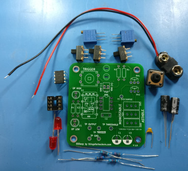
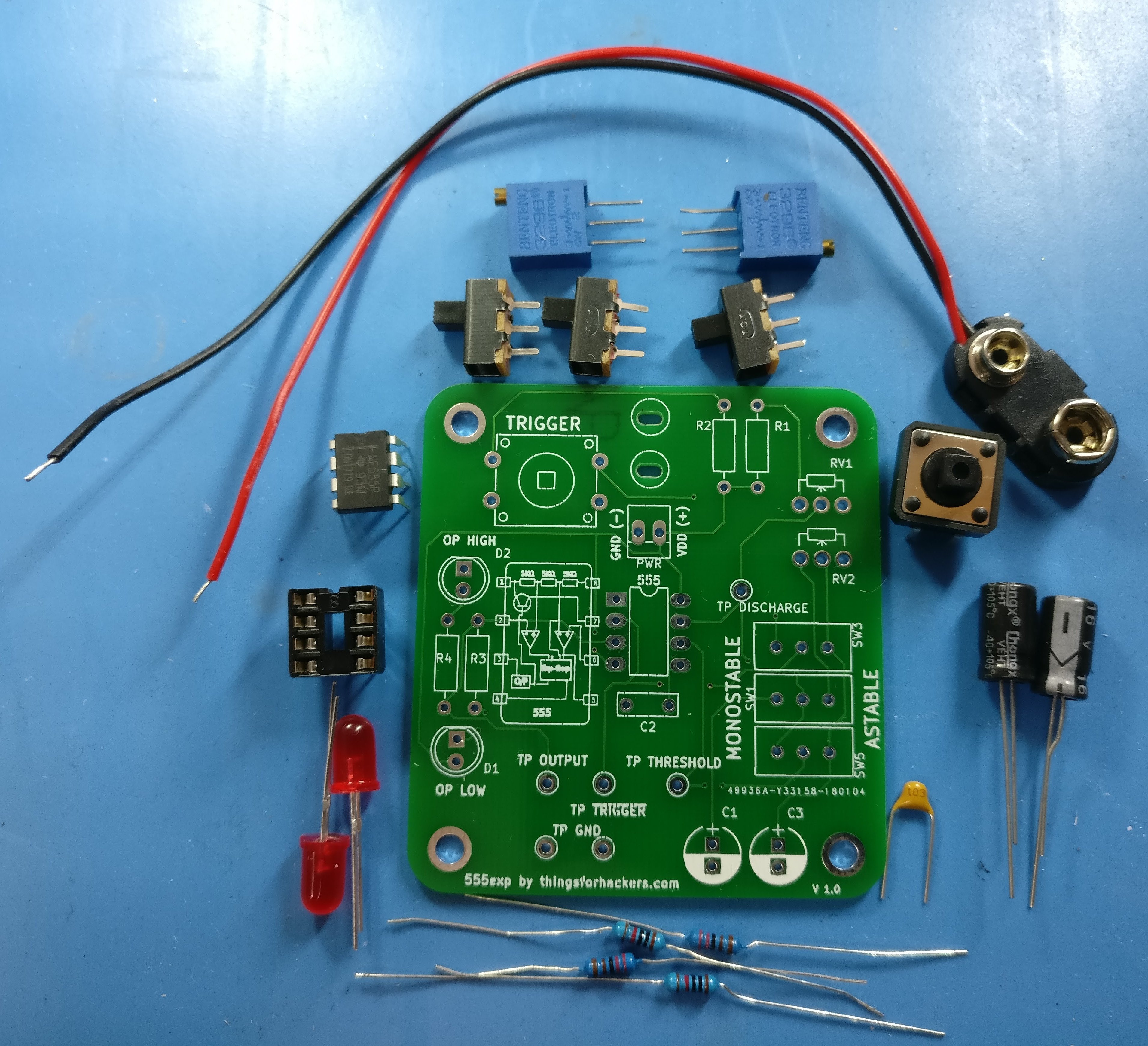
Kit contents
The kit contains the following:
- 1 * 555exp PCB
- 1 * 555 timer IC (with socket)
- 2 * 470uF electrolytic capacitors
- 1 * 10nF ceramic capacitor
- 2 * 5mm red L.E.Ds
- 1 * 10KΩ resistors
- 1 * 1KΩ resistor
- 2 * 2K2Ω resistors
- 2 * 0-10KΩ variable resistors
- 3 * SPDT slide switches
- 1 * push to make tact switch
- 6 * test point rings
- 1 * PP3 battery cable
What you will need
The following is a list of tools that will be required to complete the build:
- A soldering Iron
- Some solder
- A pair of thin nosed pliers
- A pair of side cutters
Optionally, these might make things a bit easier for you:
- Some sort of desk top clamp
- Magnifying glass if you struggle with fine detail
In addition you will need to source a PP3 or equivalent 9V battery.
Build Steps
For somebody who’s soldered before, the build should take about 15 mins or so.
In general, the easiest build process is to start with the lowest (in terms of height) components first, this allows you to insert the part, turn over the board and solder without the part falling off of the board to much. With that in mind, I suggest the following order:
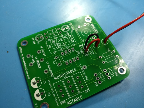
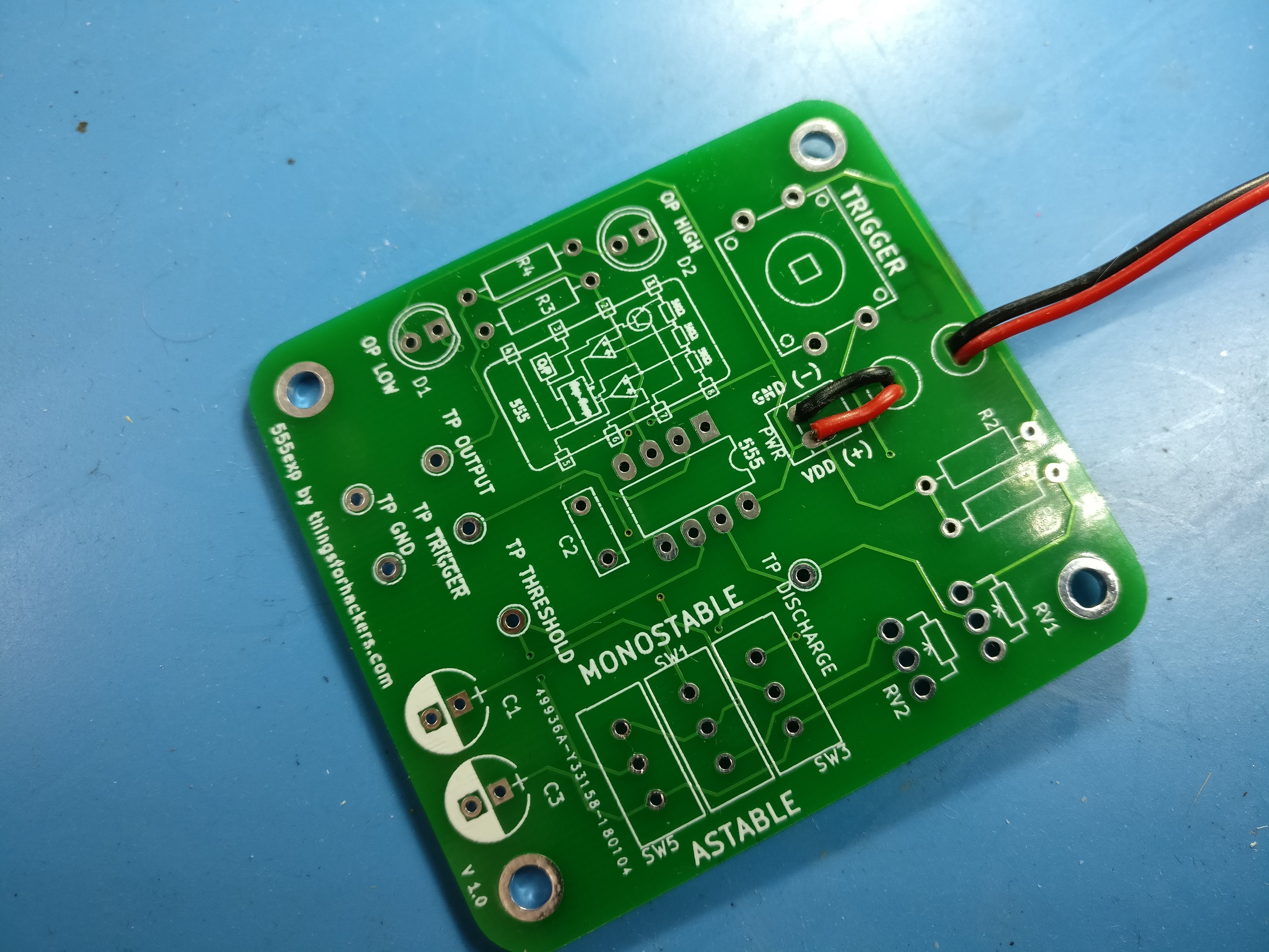
1. PP3 battery cable
The cable should be threaded through the strain relief holes as shown in the following image. Please ensure red goes to the VDD (+) pad and black to GND (-).
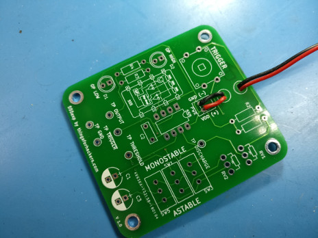
Once you have the cable as shown, turn the board over and solder. Then carefully pull the cable tight, once done it should look as follows:
2. Fixed value resistors R1, R2, R3 & R4
Using the thin noise pliers, form each resistor in to a U shape. Try and make the legs about 1cm apart. It doesn’t matter which way round the resistors go, but the values are not all the same:
- R1 (1KΩ)
- Brown, Black, Black, Brown
- R2 (10KΩ)
- Brown, Black, Black, Red
- R3 & R4 (2K2Ω)
- Red, Red, Black, Brown
3. Test point pins (Optional)
As an optional step, you can fit the 6 test point rings. These are not needed to proper operation, but can be used to connect an oscilloscope or other test equipment if so desired.
4. Capacitor C2
C2 is slightly below the middle of the board, it can go either way round.
5. Push switch SW2
The push to make tact switch can be fitted either way round. I would suggest using some thin nose pliers to straighten the legs, this will make it easier to fit.
6. 8 pin DIP socket
The 8 pin DIP socket goes in the middle of the board. Note the notch at one end, this should face towards the top of the board as shown by the pattern on the board.
7. Red LEDs D1 & D2
Both LEDs are the same, but it’s important that they are fitted the correct way round. If you look carefully at each LED, you can see that one side is slightly flattened, this should match the pattern on the board.
8. Slide switches SW1, SW3 & SW5
The three slide switches can be fitted either way round.
9. Capacitors C1 & C3
These are two 470uF electrolytic capacitors, it is very important that this are fitted the correct way around. The negative led is identified by a white strip down one side of its body, this should line up with the white shaded area on the board.
10. Variable resistors RV1 & RV2
These are located on the upper left hand side of the board. They are both the same value, but should be fitted with the turn screw on the outside of the board.
11. 555 Timer IC
Finally, carefully insert the 555 Timer IC in to the 8 pin DIP socket. The notch at the top of the IC should line up with that of the socket, and be at the top of the board.
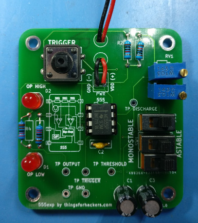
Usage Instructions
For correct operation please ensure all mode switches are moved together. I.e. they should all be fully left or fully right. Other combinations of positions are invalid.
As this circuit uses fixed value capacitors, you change the timing by adjusting RV1 & RV2.
Both RV1 & RV2 can be varied between 0 to 10KΩ.
As a rough guide:
- 1 complete clockwise turn will reduce the value by about 500Ω
- 1 complete anti-clockwise turn will increase the value by about 500Ω
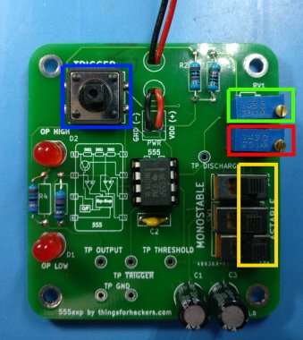
To help you identify the adjustments:
- RV1 is outlined in green.
- RV2 is outlined in red.
- Mode selection switches SW1, SW3 & SW5 are outlined in yellow.
- Slide right for Astable
- Slide left for monotstable
- The trigger button is outlined in blue
Astable mode
To enable Astable mode slide all three switches (highlighted in yellow) to the right.
When in Astable mode the output LEDS will alternately flash. The timing can be controlled by RV1 (outlined in green) & RV2 (outlined in red).
Monostable mode
To enable Monostable mode slide all three switches (highlighted in yellow) to the left.
The steady state is for the output to be low. This is indicated by LED D1 on & LED D2 off.
A quick press of the Trigger button will trigger the circuit, this will cause LED D1 to switch off & LED D2 to switch on.
The duration that D2 stays on can be adjusted with RV1.
comments powered by Disqus